Appearance
3.4 — Memory Technologies
A flip-flop from Chapter 3.3 stores one bit and costs about twenty transistors. A phone holds eight gigabytes of working memory and 256 gigabytes of storage. Twenty transistors per bit would be 10^{12} transistors for the RAM alone, which is roughly twenty times what a large processor contains.
So memory is not built from flip-flops. Every memory technology is an answer to the question: what is the least you can get away with per bit? The answers differ, and every difference you notice as a user — why RAM is fast but forgets, why SSDs wear out, why a BIOS setting survives a power cut — comes from the cell.
1. SRAM — six transistors, and it never forgets while powered
Static RAM stores each bit in a cross-coupled inverter pair, which is exactly the latch of Chapter 3.3 with the gating reduced to the minimum. Two inverters facing each other (four transistors) plus two access transistors connecting the cell to the bit lines. Six transistors per bit.
Reading. Precharge both bit lines to half the supply, then turn on the access transistors. The cell's inverter pulls one bit line slightly one way, and a sense amplifier detects the tiny difference and amplifies it to a full logic level. The cell is disturbed but not destroyed, so no rewrite is needed.
Writing. Drive the bit lines hard to the wanted value and turn on the access transistors. The drivers overpower the cell's own inverters and flip it. The access transistors must be strong enough to write but weak enough not to disturb the cell during a read — that balance is called the cell ratio, and getting it right at small geometries is one of the hardest parts of chip design.
Properties. Access time under 1 ns on-chip. No refresh needed. Zero standby current apart from leakage. And volatile — cut the power and the inverter pair has nothing to hold it, so the value is gone in microseconds.
Where it lives: every processor cache (L1, L2, L3), every register file, every FPGA's internal block RAM, and the small buffers inside every peripheral. Volume I, Chapter 1.6 describes what the caches do with it; this is the cell they are made of.
Why not use it for main memory? Six transistors per bit against DRAM's one. SRAM costs roughly six times the silicon area per bit, and area is money. That is the entire reason the memory hierarchy exists.
What those six transistors actually look like
Six transistors sounds like a lot for one bit until you see how they are arranged, because four of them are doing one job and two are doing another.
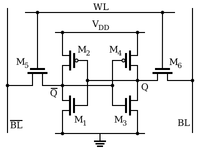
The middle four are two inverters facing each other, each one's output feeding the other's input. Suppose the left node is high. That drives the right inverter's input high, so its output goes low, which drives the left inverter's input low, so its output goes high — which is where we started. The ring holds itself. It is a loop of two NOT gates, and a loop of two NOT gates has exactly two stable states, which is why it stores one bit and why the cell needs no refreshing.
The outer two are access transistors, one on each side, both switched by the word line. Raise the word line and the cell is connected to the two bit lines; drop it and the cell is sealed off and left to hold its value. That is the whole read-and-write mechanism.
Now compare the cost. Six transistors per bit is why SRAM is fast and expensive and why a processor has megabytes of cache rather than gigabytes. The next section shows what happens when you get greedy and try to do the same job with one.
2. DRAM — one transistor, and it leaks
Dynamic RAM stores each bit as charge on a tiny capacitor, with a single transistor to connect it to the bit line. One transistor and one capacitor per bit, which is as few as anyone has managed.
The capacitor is around 25 femtofarads — 25\times10^{-15} F. Charged to 1 V, from Q = CV that is 2.5\times10^{-14} coulombs, or about 150,000 electrons. That is the entire physical representation of one bit in your computer's memory.
Reading destroys the data. Turn on the access transistor and the cell's tiny charge shares with the bit line's much larger capacitance, producing a voltage change of only tens of millivolts. A sense amplifier detects it, and then writes the value straight back, because the read has flattened it. Every DRAM read is internally a read-modify-write.
And it leaks. The access transistor's off-state leakage and the capacitor's own junction leakage drain the charge in tens of milliseconds. So every row must be read and rewritten periodically — the refresh cycle, typically every 64 ms, which is where "dynamic" in the name comes from.
Refresh costs both power and availability: while a row is being refreshed it cannot be accessed. On a modern chip this consumes a few percent of the bandwidth, and in a laptop's idle state, refresh is a real fraction of the memory subsystem's power.
The address is sent in two halves — row then column — over the same pins, which halves the pin count of a chip that would otherwise need dozens more. That is why DRAM timing has separate row and column parameters (RAS and CAS), and why accessing a new row costs more than accessing another column in the row already open. This is the hardware reason that sequential memory access is faster than random access, the fact that Volume I, Chapter 1.6 builds cache-friendly programming on.
The DDR generations
Synchronous DRAM added a clock so the chip and the controller stay in step. Double data rate transfers on both the rising and falling clock edges, doubling throughput without doubling the clock.
Each generation since has doubled the prefetch: the internal array runs at a modest speed, but each internal access fetches 8 or 16 bits per pin at once and the interface serialises them at high speed. The array has barely got faster in twenty years; the interface has got much wider and much faster. That is why memory latency has improved so little while bandwidth has improved enormously, and it is the deep reason caches matter more every year.
3. Read-only and programmable memories, in historical order
Mask ROM. The data is built into the chip's wiring during manufacture. Cheapest per bit at high volume, impossible to change, and a fab run takes weeks. Used for anything shipped in millions and never updated.
PROM. Ships blank with a fusible link at every cell; programming blows the chosen fuses with a high current. One shot, permanently.
EPROM. A floating gate transistor — a second gate completely surrounded by insulator, sitting between the control gate and the channel. Trap electrons on it and they shift the transistor's threshold voltage (Chapter 2.4), so the cell reads as 0 rather than 1. Since the gate is surrounded by insulator, the charge stays for decades.
Erasing needed ultraviolet light through a quartz window in the package, which gave the electrons enough energy to escape the insulator. Twenty minutes under a UV lamp erased the whole chip. Anyone who worked with 1980s hardware remembers the sticker over the window, because ordinary sunlight would slowly erase it.
EEPROM. Same floating gate, but erasable electrically, and byte by byte. Convenient and expensive in area, because each byte needs its own erase circuitry.
Flash. EEPROM's insight applied at scale: erase in large blocks rather than per byte, which removes most of the per-cell circuitry and drops the cost per bit enormously. That single compromise created the entire memory-card, SSD and phone-storage industry.
4. Flash in detail
Writing ("programming") uses either hot-carrier injection or Fowler-Nordheim tunnelling to push electrons onto the floating gate. It can only turn a 1 into a 0.
Erasing removes the electrons, restoring all bits to 1, and can only be done a whole block at a time — typically 128 KB to several megabytes.
That asymmetry is the origin of every strange behaviour of flash storage. You cannot overwrite a byte in place: you must erase the whole block containing it and write it back. So the controller instead writes the new data somewhere else, marks the old copy invalid, and later reclaims blocks whose contents are mostly invalid. That is garbage collection, and it is why an SSD's write speed drops when it is nearly full — there are fewer free blocks to write into and more work to reclaim one.
NOR versus NAND
NOR flash connects each cell in parallel to the bit line, so any byte can be read directly. Random access, fast reads, slow writes, expensive per bit. Used for code that must run directly from flash — a microcontroller's program memory, a BIOS.
NAND flash connects cells in series strings, which is far denser but means you cannot read one cell without the whole string. Access is by page (a few kilobytes) rather than by byte. Cheap, dense, slower random access. Everything you think of as "storage" is NAND.
Wear
Every erase pushes electrons through the insulating oxide, and each passage damages it slightly. Eventually the trapped charge cannot be reliably distinguished and the block fails.
| Cell type | Bits per cell | Voltage levels | Endurance |
|---|---|---|---|
| SLC | 1 | 2 | ~100,000 cycles |
| MLC | 2 | 4 | ~10,000 |
| TLC | 3 | 8 | ~3,000 |
| QLC | 4 | 16 | ~1,000 |
Storing more bits per cell means distinguishing more voltage levels on the same floating gate. QLC must resolve sixteen distinct charge levels, so the margin between them is a sixteenth of what SLC enjoys, and any drift or damage crosses a boundary much sooner. That is the whole trade: capacity for endurance and speed.
Wear levelling is the controller's answer — spread writes evenly across all blocks so no single block is exhausted while others are untouched. Combined with over-provisioning (spare blocks the user cannot see) and error correction, a modern TLC SSD survives hundreds of terabytes written, which is far beyond ordinary use.
Charge does eventually leak, which is why a flash drive left unpowered for several years can lose data, and why the JEDEC retention specification for a worn consumer SSD is one year at 30 °C. This is worth knowing before treating an SSD as archival storage.
5. The newer non-volatile memories
Flash's problems — block erase, wear, slow writes — motivated a long search for something better.
FRAM uses a ferroelectric crystal whose polarisation direction stores the bit. Writes are as fast as reads, endurance is 10^{14} cycles, and power is tiny. Density is poor and cost is high, so it appears in smart meters and medical devices where a decade of frequent writes matters more than capacity.
MRAM stores the bit in the magnetic orientation of a thin layer, read through the tunnel magnetoresistance effect. Non-volatile with SRAM-like speed and unlimited endurance. It is now replacing embedded flash in some microcontrollers and is used for cache backup.
3D XPoint (Optane) used a resistance change in a chalcogenide material, sitting between DRAM and flash in both speed and cost. Technically successful, commercially not — it was discontinued in 2022, which is a useful reminder that a technology can be genuinely better on the specification sheet and still lose to economics.
The deeper point: DRAM and NAND have had four decades of manufacturing volume driving their cost down. A newcomer must beat not just their physics but their learning curve, and almost nothing does.
6. How a memory chip is organised
Not as a long line of bits — as a two-dimensional array.
A 1 megabit chip is built as 1024 rows by 1024 columns. The address is split: 10 bits choose a row through a decoder (Chapter 3.2), and the whole row is read into sense amplifiers at once; the other 10 bits choose which of those 1024 bits to send out.
Why square? A 1-megabit linear array would need a 1-to-1,048,576 decoder — a million AND gates. Two 1-to-1024 decoders need about two thousand. The square organisation reduces the decoder from 2^n to 2\cdot2^{n/2}, which is the difference between possible and not.
It also explains the row-access behaviour of section 2: once a row is in the sense amplifiers, further accesses to that row are nearly free, while a different row costs a full array access. The memory chip has an accidental cache of one row, and DRAM controllers work hard to exploit it.
Building wider and deeper
To get more bits per word, put chips in parallel: eight 1-bit-wide chips sharing the same address lines give an 8-bit word. To get more addresses, use a decoder on the high address bits to generate chip selects, exactly as Chapter 3.2 described. Every memory module ever made is one of these two arrangements or both.
7. Error detection and correction
At these scales, errors are not hypothetical. A cosmic ray secondary particle or an alpha particle from trace radioactivity in the package can deposit enough charge to flip a DRAM cell. Rates of roughly one error per gigabyte per month are typical at sea level, and higher at altitude.
Parity adds one bit per byte, set so the total number of 1s is even. It detects any single-bit error and cannot correct anything. Cheap, and it turns silent corruption into a visible fault, which is a real improvement.
Hamming ECC adds enough bits to identify which bit failed. For 64 data bits, 8 check bits give SECDED — single error correction, double error detection. Volume I, Chapter 1.8 develops the coding mathematics; the hardware cost is 12.5% extra memory and a few nanoseconds of latency.
Server memory has ECC and consumer memory usually does not, purely on cost. The consequence is that a consumer machine silently corrupts data occasionally and a server does not, which matters enormously for a database and not at all for a game.
Rowhammer deserves a mention because it is a genuine physical attack: repeatedly activating one DRAM row couples enough disturbance into the physically adjacent rows to flip their bits, without ever accessing them. It turns a memory density limit into a security vulnerability, and mitigations — targeted refresh, ECC, activation counting — have been an arms race since 2014.
8. Choosing, in one table
| Need | Use | Because |
|---|---|---|
| Processor cache | SRAM | fastest, no refresh |
| Main memory | DRAM | cheapest per bit that is fast enough |
| Code that runs in place | NOR flash | random read access |
| Bulk storage | NAND flash | cheapest non-volatile |
| Settings written constantly | FRAM or EEPROM | endurance |
| Data that must survive power loss | any non-volatile | volatile loses it in microseconds |
The memory hierarchy of Volume I, Chapter 1.6 is exactly this table sorted by speed. The reason such a hierarchy has to exist at all is one sentence: no single technology is simultaneously fast, dense, cheap and non-volatile.
Every level is a different compromise between those four. And because the fast levels are the small expensive ones, a computer's design becomes the art of making them appear larger than they are — which is what caching, prefetching and virtual memory are all doing.
Every technology in this chapter stores discrete values, which is the whole premise of Part 3. The next chapter is where the digital world meets the analog one it lives inside, and where a continuous voltage is turned into a number and back again.
Every formula above, built from scratch
None of the results in this chapter are worth memorising, because each one can be rebuilt in under a minute from something simpler. What follows is that rebuilding, one result at a time, so the formula and the reason for it sit on the same page as the explanation that needed them.
Memory
Cell costs: SRAM 6 transistors; DRAM 1 transistor + 1 capacitor; flash 1 transistor.
Q_{cell} = C_{cell}V
At 25 fF and 1 V: 2.5\times10^{-14} C, about 150,000 electrons per bit.
Array organisation: 2^n bits as 2^{n/2} rows by 2^{n/2} columns, needing 2\cdot2^{n/2} decoder outputs instead of 2^n.
\text{address bits} = \log_2(\text{locations}), \qquad \text{total bits} = \text{locations}\times\text{width}
Hamming code, for k data bits the number of check bits r must satisfy
2^r \ge k+r+1
For k=64: r=7 for correction, plus one more for double-error detection, giving the familiar 72 bits per 64.