Appearance
3.6 — Microcontrollers and FPGAs
You need to blink an LED when a button is pressed. You could wire a flip-flop. You could write four lines of C on a chip costing thirty cents. You could describe the logic in a hardware language and configure an FPGA.
All three work. What separates them is not capability but where the design lives — in copper, in instructions, or in a configuration bitstream — and the choice determines cost, speed, power and how long the next change takes.
Everything in this chapter is built from the flip-flops of Chapter 3.3 and the combinational blocks of Chapter 3.2, in quantity. The only genuinely new idea is that the wiring between them can be decided after the chip is manufactured.
1. Microprocessor, microcontroller, SoC
A microprocessor is a CPU and little else. It needs external memory, external peripherals and a support chipset. Desktop and server processors are these.
A microcontroller is a CPU plus its memory plus its peripherals on one chip. Flash for the program, SRAM for variables, timers, ADC, serial ports, general-purpose pins. Add a crystal and a decoupling capacitor and it runs. It is a complete computer sold for under a euro.
A system on chip is the same idea scaled up: several CPU cores, a graphics processor, a memory controller, radios and video engines, all on one die. A phone's main chip is this.
The distinction that matters is what you are buying. A microprocessor is bought for computing throughput. A microcontroller is bought for its peripherals and its determinism — the CPU is often the least interesting part.
What "programmable hardware" actually means
The phrase suggests something mysterious. It is not. An FPGA is a field of very small identical blocks, and one of them looks like this.
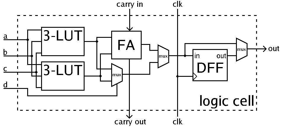
The lookup table is the trick. It is a tiny memory, typically holding 16 bits, addressed by the cell's four inputs. Whatever four-input Boolean function you want, you do not build it from gates — you write out its truth table and store it. Want AND? Store a 1 in the one row where all four inputs are high and 0 everywhere else. Want XOR? Store the XOR truth table. The same silicon becomes any four-input gate depending only on sixteen bits of configuration, and that is what "programmable hardware" means.
The flip-flop gives the cell the option of remembering its output rather than just computing it, which is what lets you build sequential logic (Chapter 3.3) rather than only combinational.
The multiplexer picks between the two, so one cell type covers both needs.
Now multiply by a hundred thousand cells and add a programmable grid of wires between them, and you can wire up any digital circuit that fits — a processor, a video decoder, twenty independent counters — by loading a configuration file. That is the difference from the microcontroller in section 1: the microcontroller runs your instructions one after another on fixed hardware, and the FPGA becomes hardware that does your job all at once.
2. Inside a microcontroller
Volume I, Chapter 1.5 covers how a CPU executes instructions. What follows is what surrounds it, because that is where embedded work actually happens.
Program memory — flash, typically 8 KB to 2 MB. Code executes directly from it (NOR flash, Chapter 3.4).
Data memory — SRAM, typically 1 KB to 512 KB. Variables and stack.
The two are separate address spaces on a Harvard architecture (most microcontrollers) and one shared space on a von Neumann one. Harvard lets an instruction fetch and a data access happen simultaneously, which is worth a real speed increase without a cache.
The peripherals, each of which solves one problem
GPIO — general purpose input/output pins. Each is individually configurable as input or output, with an optional internal pull-up or pull-down resistor (removing the need for an external one), and configurable drive strength and slew rate. The slew rate control matters more than it sounds: a fast edge radiates interference, so slowing down every pin that does not need to be fast is a real fix for a board that fails electromagnetic compliance testing.
Timers/counters. The most-used peripheral. A counter clocked by the system clock or an external signal, with compare registers that trigger an interrupt or toggle a pin at a chosen count. From this one block you get:
- PWM — set the period in one register and the duty in another. Drives motor speed, LED brightness, and the servo signal every hobby robot uses.
- Input capture — record the counter value when a pin changes, which measures pulse widths and frequencies precisely.
- Periodic interrupt — the tick that every real-time operating system schedules on.
ADC — successive approximation, 10 or 12 bits, with a multiplexer so one converter serves many pins (Chapter 3.5).
Communication peripherals, which deserve their own comparison since choosing between them is a real design decision:
| UART | SPI | I²C | CAN | |
|---|---|---|---|---|
| Wires | 2 | 4 + 1 per device | 2 | 2 |
| Clock | none, agreed rate | shared | shared | none |
| Speed | to 1 Mbit/s | 50 Mbit/s+ | 0.1–3.4 Mbit/s | 1 Mbit/s |
| Devices | 2 | many, one select each | 128 by address | many |
| Distance | metres | centimetres | centimetres | 40 m+ |
UART is asynchronous: no clock wire, so both ends must already agree on the bit rate. The receiver finds the start bit's falling edge and samples in the middle of each subsequent bit. It works only because the two clocks stay close enough over the ten bits of one character — about 2% tolerance — which is why UARTs need a crystal and often fail on chips using an internal RC oscillator.
SPI is synchronous and fast, with a clock line, two data lines and a separate select line per device. Full duplex, dead simple, and it costs a pin per peripheral.
I²C uses two wires with open-drain outputs and pull-up resistors — the wired-AND arrangement of Chapter 3.1. Devices are addressed rather than selected, so any number share the same two wires. Slower, and its pull-up resistors and bus capacitance set the maximum speed, exactly as computed in Chapter 3.1.
CAN was designed for cars: differential, robust, with priority-based arbitration where the lowest message ID wins without any collision or retry. When two nodes transmit at once, the one sending a dominant bit overwrites the other, and the loser detects the mismatch and simply stops — no data is lost and no time is wasted. It is a genuinely elegant protocol and it is in every vehicle built since the mid-1990s.
Watchdog timer. A counter that resets the chip unless the software regularly clears it. If the program hangs, the watchdog fires and the system restarts. Every product that must not need a person to unplug it has one, and the discipline is to clear it only from the main loop after confirming the important tasks all ran — clearing it from inside a timer interrupt defeats the purpose entirely, since the interrupt keeps running while the main program is stuck.
DMA. Direct memory access moves data between a peripheral and memory without the CPU. Set up a source, a destination and a length, and the DMA controller does the transfers while the processor does something else or sleeps. This is how a microcontroller streams audio or drives a display at all, since doing it byte by byte in software would consume the whole processor.
3. Interrupts
The mechanism that makes a microcontroller responsive.
The sequence when an interrupt fires: the current instruction finishes, the program counter and status register are pushed onto the stack, the processor jumps to a handler address taken from a vector table, the handler runs, and a return-from-interrupt instruction restores everything.
Interrupt latency is the time from the event to the first handler instruction, typically 12 to 20 cycles. Jitter in that latency matters more than its average for anything timing-critical, and the main source of jitter is a long instruction that cannot be interrupted, or a section of code that has disabled interrupts.
The rules that prevent the classic bugs
Keep handlers short. Set a flag, copy one value, and return. Do the work in the main loop. A long handler blocks every other interrupt and destroys the timing of the whole system.
Any variable shared between a handler and the main code must be declared volatile, or the compiler will cache it in a register and never notice the handler changed it. This produces a program that works at low optimisation and breaks at high optimisation, which is a genuinely nasty way to lose a day.
Multi-byte shared variables need protection. A 32-bit counter updated in an interrupt and read in the main loop can be read half-updated, giving a value that never existed. Disable interrupts briefly around the read, or read it twice and compare.
Priorities and nesting. Higher-priority interrupts can pre-empt lower ones. Useful, and it means the stack must be deep enough for the worst-case nesting — a stack overflow in an embedded system does not throw an exception, it silently overwrites variables.
4. Real-time behaviour, and what "real-time" means
A real-time system is one where being late is being wrong. It does not mean fast.
Hard real-time: a missed deadline is a failure. An airbag controller, a motor commutation loop, an engine's ignition timing.
Soft real-time: a missed deadline degrades quality. Audio playback, a user interface.
The important consequence is that a hard real-time system must be analysable in the worst case, not the average case. That rules out things whose timing you cannot bound: dynamic memory allocation, caches with unpredictable hits, and any operating system that does not guarantee a maximum latency.
A real-time operating system provides pre-emptive priority scheduling with bounded latency, so the highest-priority ready task runs within a known time. The bug it introduces is priority inversion: a low-priority task holds a lock that a high-priority task needs, and a medium-priority task then pre-empts the low one, so the high-priority task waits indefinitely for something a medium task is blocking. The fix is priority inheritance — the lock-holder temporarily inherits the priority of the highest task waiting for it.
This is not a textbook scenario. It is what stopped the Mars Pathfinder rover in July 1997, causing repeated system resets until engineers uploaded a patch enabling priority inheritance in the VxWorks mutex — from 190 million kilometres away.
5. Power, the constraint that shapes battery-powered design
A sensor that must run three years on a coin cell has a budget of roughly:
\frac{220\ \text{mAh}}{3\times365\times24\ \text{h}} = 8.4\ \mu\text{A average}
A microcontroller running flat out draws 5 to 20 mA. So it must be asleep more than 99.9% of the time.
The sleep modes, in a typical part:
| Mode | Current | Wakes on | Wake time |
|---|---|---|---|
| Run | 10 mA | — | — |
| Sleep | 2 mA | any interrupt | instant |
| Stop | 5 µA | pin or watchdog | tens of µs |
| Standby | 0.3 µA | pin or alarm | ms, restarts |
The design pattern: wake on a timer, take a reading, transmit if needed, sleep again. Duty cycling is everything.
Worked example. A sensor waking every 60 s, awake for 10 ms at 8 mA, sleeping at 2 µA:
I_{avg} = 8\ \text{mA}\times\frac{0.01}{60} + 2\ \mu\text{A} = 1.33\ \mu\text{A}+2\ \mu\text{A} = 3.33\ \mu\text{A}
\text{Life} = \frac{220\ \text{mAh}}{3.33\ \mu\text{A}} = 66{,}000\ \text{hours} = 7.5\ \text{years}
Notice that the sleep current dominates. Halving the active time saves 20%; halving the sleep current saves 30%. That is why datasheets fight over nanoamps in standby, and why one forgotten pull-up resistor drawing 30 µA can cut a design's life by a factor of ten. Always compute the average, and always check what every resistor on the board is doing while asleep.
6. FPGAs
A field-programmable gate array is a chip full of generic logic that you configure into whatever circuit you want, after manufacture. The name is literal: the gates are arranged in an array, and they are programmable in the field.
What is actually inside
Logic blocks, each containing:
- A lookup table — a small memory, usually 6 inputs and 1 output, holding 64 bits. Load those bits with any truth table and the LUT becomes that function. This is the multiplexer-as-universal-gate idea from Chapter 3.2, made real: a 6-input LUT can be any function of 6 variables, so there is no need for a library of different gate types.
- A flip-flop, so the block can be sequential.
- Fast carry logic, because adders are so common that dedicated carry chains are worth the silicon.
Programmable interconnect — a switching fabric of wires and configurable connections between blocks. This is most of the chip's area and most of its delay, and routing congestion, not logic capacity, is usually what stops a design fitting.
Hard blocks — full-custom circuits included because they are used constantly and would be wasteful in generic logic: block RAM (tens of kilobits each), DSP slices (a multiplier plus an accumulator), clock managers with PLLs, high-speed serial transceivers, and sometimes complete processor cores.
Configuration memory — SRAM cells holding every LUT's contents and every routing switch's state. Being SRAM, it is volatile: the FPGA loads its configuration from an external flash chip at every power-up, taking tens to hundreds of milliseconds. Some families use flash or antifuse configuration instead and start instantly.
The design flow, and why it is slow
- Describe the hardware in VHDL or Verilog, or increasingly with high-level synthesis from C.
- Simulate, because debugging in simulation is a hundred times easier than on the board.
- Synthesise — the tool converts your description into a netlist of LUTs, flip-flops and hard blocks. This is where Chapter 3.1's Boolean minimisation happens, done by algorithms far better than a person.
- Place and route — decide which physical block does what, and find wire paths between them. This is the slow step, taking minutes to many hours, because it is a large optimisation problem with timing constraints.
- Timing analysis — verify that every path meets the setup and hold equations of Chapter 3.3, at worst-case temperature and voltage.
- Generate the bitstream and load it.
A one-line change requires the whole flow again, which is why FPGA development has a rhythm completely unlike software. It is also why simulation is not optional.
An important warning about hardware description languages
VHDL and Verilog look like programming languages and are not. You are describing a circuit, not a sequence of steps. Every statement in a hardware description happens simultaneously, all the time, because it is wire and gates. Writing what appears to be a loop creates n copies of the hardware, not n iterations in time.
The first thing an engineer coming from software must unlearn is sequential thinking. The tell-tale symptom is a design that simulates as intended and synthesises into something enormous, because every apparent "variable assignment" became another physical register.
7. FPGA versus microcontroller versus custom chip
| Microcontroller | FPGA | ASIC | |
|---|---|---|---|
| Design cost | very low | medium | millions |
| Unit cost | €0.30–€10 | €10–€10,000 | pennies at volume |
| Change after shipping | firmware update | bitstream update | new mask set |
| Parallelism | one thing at a time per core | genuinely unlimited | genuinely unlimited |
| Timing determinism | good | exact | exact |
| Power per operation | medium | high | lowest |
| Time to first working thing | hours | weeks | a year |
Choose a microcontroller when the task is sequential, timing needs are in microseconds, and you want to be finished this week. This is most of the time.
Choose an FPGA when you must do many things genuinely at once, or handle data faster than any processor can — video processing, software-defined radio, high-frequency trading, protocol bridging, or interfacing to hardware whose timing no processor could meet. Also when the volume is too low to justify a custom chip.
Choose an ASIC only at very high volume, or when nothing else meets the power or speed requirement. The mask set alone costs millions and there is no second chance.
Worked comparison
Task: multiply two 16-bit numbers, 100 million times per second.
- Microcontroller at 100 MHz with a single-cycle multiplier: 100 million multiplies per second, using 100% of the processor and leaving nothing for anything else. Just barely, and only if it does nothing else at all.
- FPGA: one DSP slice does one multiply per clock. At 200 MHz that is 200 million from a single slice, and a mid-range part has a thousand slices. 200 billion per second, and you have used 0.1% of the chip.
- The gap is a factor of two thousand, and it exists entirely because the FPGA does things in parallel while the processor does them in sequence.
Now change the task: parse a JSON configuration file. The microcontroller does it in a few lines. The FPGA needs a state machine of hundreds of states and weeks of work. Sequential, branching, irregular work is what processors are for, and no amount of parallel hardware helps.
That contrast is the whole decision, and it is the same one that separates a CPU from a GPU in Volume I, Chapter 12.9.
Part 3 has treated signals as sequences of discrete values without asking what a signal is or what a circuit does to it in general. Part 4 answers both, and its tools — convolution, Fourier, Laplace — are the mathematical backbone of everything that follows in this volume.
Every formula above, built from scratch
None of the results in this chapter are worth memorising, because each one can be rebuilt in under a minute from something simpler. What follows is that rebuilding, one result at a time, so the formula and the reason for it sit on the same page as the explanation that needed them.
Microcontroller sizing
I_{avg} = I_{active}\cdot D + I_{sleep}(1-D), \qquad D = \frac{t_{active}}{t_{period}}
\text{battery life} = \frac{\text{capacity (mAh)}}{I_{avg}\ (\text{mA})}
PWM:
\text{duty} = \frac{t_{on}}{T}, \qquad V_{avg}=D\cdot V_{supply}, \qquad \text{resolution bits} = \log_2\frac{f_{timer}}{f_{PWM}}
That last one is the constraint people hit: a 48 MHz timer producing 20 kHz PWM gives 48\times10^6/20\times10^3 = 2400 steps, which is 11.2 bits. Ask for 16-bit PWM at 20 kHz and you need a 1.3 GHz timer.
UART timing:
t_{bit} = \frac{1}{\text{baud}}, \qquad \text{frame} = 1 \text{ start}+n\text{ data}+\text{parity}+\text{stop bits}
\text{throughput} = \text{baud}\times\frac{n_{data}}{n_{frame}}
At 115200 baud with 8N1 (10 bits per byte): 11,520 bytes per second.
Clock tolerance: the receiver samples the last bit of a 10-bit frame after 9.5 bit times, so an accumulated error must stay under half a bit — about 5% total between the two ends, and in practice 2% each is the working limit.
I²C pull-up:
t_{rise}=0.8473\,R_pC_{bus} \quad(\text{30\% to 70\% per the specification}), \qquad R_{p(min)}=\frac{V_{DD}-V_{OL}}{I_{OL}}
Sixteen worked problems next.
What the next chapter fixes
Part 3 has treated signals as strictly two-valued, which is a convenient fiction that ends at the boundary of any real system. Sound, light, temperature and radio are continuous, and Part 4 develops the mathematics for handling them: what a signal actually is, what makes a system predictable enough to analyse, and the transforms that turn hard problems in time into easy ones in frequency.